PCB Design - How CAD
Software Transforms
Ideas into Reality
In our digital age, every gadget - from smartphones to satellites - relies fundamentally on one powerhouse element: the printed circuit board.
Top 5 Beginner PCB Design Mistakes (and how to fix them)

Exploring PCB Design:
Understanding the Basics
Delve into the world of Printed Circuit Board (PCB) design, a cornerstone of modern electronics. This guide unravels the fundamentals, from understanding what PCBs are and exploring their various types to unveiling the intricate processes behind their creation and identifying key players in the design ecosystem.

PCB Design
Process
Printed Circuit Board (PCB) design underpins the functionality and reliability of modern electronics.

PCB designers are the engineers who design Computer-Aided Design (CAD) drawings of PCBs to meet a range of engineering requirements, and they prepare PCBs for manufacturing at scale.
This involves a range of tasks, spanning from circuit design to component placement, layout, routing, reviewing for manufacturing, and testing prototypes. More advanced tasks can involve simulating designs for signal integrity, power integrity, EMI/EMC, and RF/wireless functionality.
In many projects, alongside PCB design, firmware (FW) code development for component control significantly influences the entire device's functionality. This often determines the choice of control and controlled components, thereby having a substantial impact on the PCB design itself. Additionally, software (SW) and graphical user interface (GUI) development can be integral parts of the entire process of creating the final device.
Essential CAD
Tools for Efficient
PCB Design

Modern CAD software applications are crucial for achieving efficient and effective PCB designs. These tools provide a comprehensive suite of functionalities that streamline the design process, enabling designers to meet their goals with ease.
Key tools and
features include:
Simplifies the creation of complex circuit diagrams, ensuring accurate and efficient design.
Facilitates the physical layout of the PCB, optimizing component placement and routing.
Allows for early testing and validation of designs, reducing the need for multiple prototypes.
Ensures compliance with industry standards and design requirements, minimizing errors.
Provides a realistic view of the PCB, aiding in the detection of potential issues before manufacturing to ensure enclosure fit.
Enhances communication between designers and manufacturers, ensuring alignment and reducing time-to-market.
The Digital Thread: Connecting
Design Data to the Real World
Modern ECAD software creates a seamless digital thread between PCB designers and the factory floor, facilitating early review and inspection of design data. This collaboration is essential for:
Reducing Prototype Spins
Early detection of design issues helps minimize the number of iterations required, saving time and resources.
Improving Quality
Continuous feedback from manufacturers ensures that designs meet quality standards and functional requirements.
Optimizing Cost
Collaborative design processes help identify cost-saving opportunities, making new products more economically viable.
Easing Transition
to Volume Production
Well-documented and validated designs streamline the shift from prototyping to full-scale production, reducing lead times and enhancing efficiency.
In-House
PCB Design
vs. Outsourcing

Today’s PCB design software vendors implement collaboration and communication tools within their design environment, including secure cloud solutions that allow seamless design, procurement, and manufacturing data transfer.
In-House

Many companies that use PCBs in their products keep core engineering functions in-house while outsourcing their PCB design work to service bureaus, freelancers, and a contract manufacturer.
Bureau

PCB service bureaus offer a flexible option that can scale up or down based on customer needs. However, working with external service providers requires collaboration with internal team members and a contract manufacturer.
PCB Design Workflow
Idea

Research and Conceptualization
Define the project requirements: Determine the specifications, performance requirements, and constraints of the project.
System Design
Creating Specs and Choosing Components: Conduct research on similar projects, technologies, and components to gain an understanding of what is required for the project.
PCB Design

Creating Schematics and Simulation
Schematic design: Develop a schematic of the electronic system, including the power supply, signal conditioning, and control elements.
Material Selection, Layout, and Component Placement
PCB layout: Design the printed circuit board layout, including the placement of components, routing of signals, and consideration of noise and interference.
Component Purchasing
Procurement: Select, source, and purchase the right electronic design components.
Prototyping

DFX (Rule Checks, Thermal Simulations, & Signal Integrity)
Prototype fabrication: Create a prototype of the design to perform testing to verify the functionality and performance of the design.
Prototype Validation
Testing, Debugging, and Refinement: Create a prototype of the design to test, verify, and validate the design while refining functionality based on the results.
Design Compliance

Certification and Documentation
Production Documentation: Prepare the design for production and certification with regulatory bodies with comprehensive documentation covering requirements, fabrication, assembly, and other documentation. Perform compliance testing to ensure the design meets regulatory requirements.
Manufacturing

Production
Fabrication and Assembly: Create a prototype of the design to test and verify its functionality.
Post-Production and Sustainability
Support and maintenance: Provide ongoing support and maintenance for the product, including repairs, updates, and improvements.
Idea
Research and Conceptualization
Define the project requirements: Determine the specifications, performance requirements, and constraints of the project.
System Design
Creating Specs and Choosing Components: Conduct research on similar projects, technologies, and components to gain an understanding of what is required for the project.
PCB Design
Creating Schematics and Simulation
Schematic design: Develop a schematic of the electronic system, including the power supply, signal conditioning, and control elements.
Material Selection, Layout, and Component Placement
PCB layout: Design the printed circuit board layout, including the placement of components, routing of signals, and consideration of noise and interference.
Component Purchasing
Procurement: Select, source, and purchase the right electronic design components.
Prototyping
DFX (Rule Checks, Thermal Simulations, & Signal Integrity)
Prototype fabrication: Create a prototype of the design to perform testing to verify the functionality and performance of the design.
Prototype Validation
Testing, Debugging, and Refinement: Create a prototype of the design to test, verify, and validate the design while refining functionality based on the results.
Design Compliance
Certification and Documentation
Production Documentation: Prepare the design for production and certification with regulatory bodies with comprehensive documentation covering requirements, fabrication, assembly, and other documentation. Perform compliance testing to ensure the design meets regulatory requirements.
Manufacturing
Production
Fabrication and Assembly: Create a prototype of the design to test and verify its functionality.
Post-Production and Sustainability
Support and maintenance: Provide ongoing support and maintenance for the product, including repairs, updates, and improvements.
Altium PCB Design Solutions
Altium comes with a full set of powerful solutions
for creating outstanding PCB Designs

What is a PCB?
PCB design is the essential framework powering innovation across today’s electronic landscape.
A printed circuit board (PCB) is a one-, two-, or multiple-layer structure that interconnects electrical circuitry. The PCB layers are laminated or pressed together to form a layer stack with embedded metal surfaces called traces and larger areas of metal called planes.
Metal pads on the PCB allow the solder to hold electronic components in place using the traces and planes to interconnect circuitry to communicate signals.

Why do
we have PCBs?
From smartphones to kitchen appliances, PCBs are integral to the functionality and innovation of today's electronics. PCBs connect components in everything from essential gadgets to advanced systems. Their adaptability across various applications highlights their importance in ensuring consistent performance and systematic organization.

PCBs satisfy the demand for smaller, more advanced products because they enable the integration of diverse functions and components into a single system. In addition, many semiconductor devices, particularly advanced chips, may not function correctly if not assembled onto a precisely engineered PCB.
PCBs integrate multiple electronic functionalities onto a single board, such as:
PCBs are the primary value-creating component in nearly every electronic device. PCBs appear in a very wide range of applications from simple, universal designs to highly complex, specialized ones, underscoring their adaptability to different applications.
Altium PCB Design Solutions
Altium comes with a full set of powerful solutions
for creating outstanding PCB Designs

Types of PCBs
The most common type of PCB is a double-sided board, which has two layers of copper foil, one on each side.
Boards are composed of rigid, flex, or rigid-flex layers of insulating material—typically fiberglass FR4—with conductive pathways (commonly copper or gold) etched or deposited on the layer surface.
Tracks and planes ensure the correct flow of electricity, allowing various components, such as resistors, capacitors, and integrated circuits, to perform their designated functions in a compact, reliable, and efficient manner.

Fiberglass FR4
Board insulating material
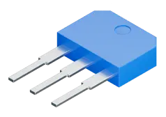
Diode
PCB component

Types of PCBs

Different types of PCBs are crafted with specific functionalities in mind—be it the flexibility needed in wearable tech or the thermal management crucial in high-power LED applications.
Understanding these variants is essential for engineers and designers to select the most suitable PCB, balancing performance, cost-efficiency, and adaptability to environmental conditions.
Precisely engineered PCBs enable specific applications varying in base materials, data rate capabilities, operating frequency range, thermal reliability, and rigidity.
To stay productive, PCB designers utilize ECAD software with specialized features that accelerate each phase of the PCB design process.
Using the right software tools makes it easy to design manufacturable boards with all the necessary design output files for prototypes or full-scale production.


.png)
Rigid PCBs are the standard in electronic design; they are crafted from solid substrate materials and provide a sturdy platform that resists bending. Due to their durability and cost-effectiveness, these PCBs are ubiquitous in everyday electronics, from personal computers to home appliances.
Flexible PCBs are made of pliable materials and offer the unique ability to bend and flex—making them a sure fit for tight spaces over traditional PCBs. This flexibility is crucial for innovative designs in modern electronics like wearable devices and foldable technology.
Rigid-flex PCBs merge the best aspects of rigid and flexible PCBs to deliver a versatile solution that combines rigid boards' durability with flex circuits' flexibility. These are ideal for complex, space-limited applications found in medical devices and aerospace technology.
Metal Core PCBs feature a metal core or metal backing, typically aluminum, for enhanced heat dissipation to address the thermal management needs of high-power electronic applications like LED lighting and automotive systems. Their design is crucial for maintaining the longevity and reliability of these applications.
PCBs used in high-frequency applications may employ materials such as RO4350B or RO4000, which are polytetrafluoroethylene (PTFE) based materials with a ceramic particle filler. These PCBs provide low loss at microwave frequencies, which is a major requirement for telecommunications and advanced radar systems where maintaining signal integrity is paramount.

Altium Designer Features for All Types of PCB Designs
Altium comes with a full set of powerful features
for creating outstanding PCB Designs

PCB Manufacturing
From smartphones to satellites, PCB design is the unifying force behind advanced electronic solutions.
All PCB designers are ultimately creating an electronic board that will be manufactured, sometimes at the scale of millions. Every PCB will need to pass important design for manufacturing (DFM) checks before it can be put into production, and passing these checks early demands collaboration with a manufacturer.

Engaging the manufacturer is often the initial step in the PCB layout creation process, and frequently, the PCB's structure is determined even before this, during the phase of gathering requirements and product specifications. This early definition is crucial for selecting the right PCB manufacturer and estimating the final cost of the laminate.
Subtractive
and Additive Manufacturing
of Printed Circuit Boards
The majority of PCBs are built with a subtractive etching process. Copper sheets are etched away from the insulating laminate material to form pads, traces, and copper pours (also called planes, regions, and polygons).

Pads

Traces

Copper pours
High Density Interconnect (HDI) and high reliability devices (Medical, Aerospace, etc.) benefit from additive manufacturing processes where copper is deposited in layers to form precise copper geometries. They are more expensive to implement, but the quality and production yield of the boards is worth the increased costs for many industries.
Once the copper geometries are complete, the layers are then pressed and bonded together into a bare circuit board. Then, solder paste is applied to the board to allow wave soldering or a reflow oven to solder Surface Mount (SMT) or Through hole components in place. The solder completes the electrical connectivity of the circuitry between components on the bare PCB, and finally, the finished boards are inspected and packaged for shipping.
From Concept
to Functional
Device

After completing the PCB design, the journey from digital blueprint to functional device begins

It starts with the manufacturing of the physical board, followed by the precise assembly of electronic components. Next, rigorous testing ensures the PCB meets all functional specifications. Any issues are corrected before the final integration into electronic devices, completing the transition from concept to operational reality.
PCB Manufacturing
The first step is PCB manufacturing, which involves producing the physical board based on the design. This process takes the design from a computer file and turns it into an actual board ready for component assembly. The manufacturing process typically starts with a base material, often a laminate, which is then processed to create the conductive paths that make up the circuit.
PCB Assembly
After the PCB is manufactured, the next step is PCB Assembly (PCBA), where all the components are placed and soldered onto the board. This step transforms the bare board into a functional PCB by adding resistors, capacitors, and integrated circuits, among other components. The assembly process involves precise placement and soldering, ensuring each component is correctly attached for the PCB to work as designed.
Testing and Quality Assurance
Once assembled, the PCB undergoes rigorous testing to ensure it functions according to its design specifications. This may include power-on tests, functionality checks, and inspections for solder quality. If any issues are found, the PCB may need to go through rework to correct the problems. Quality assurance processes are in place to guarantee that every PCB meets the required performance and reliability standards before it progresses to the final product assembly.
Final Steps
With testing and quality assurance complete, the fully assembled and tested PCBs are ready for integration into their final products, such as electronic gadgets, appliances, or industrial equipment. This final integration marks the culmination of the PCBs journey from a conceptual design to an essential component of a working electronic device.
PCB Fabrication
& Assembly Workflow
Generate Gerber Files
Export the final PCB design files in Gerber format.
Create Drill File
Prepare the drill file for vias and component holes.
Bill of Materials (BOM)
Finalize and verify the BOM with component details.
Material Selection
Choose the appropriate substrate material (e.g., FR4).
Layer Imaging
Transfer the Gerber data onto copper-clad laminate using photoresist.
Etching
Remove excess copper to create traces and pads.
Drilling
Drill holes for vias and component leads.
Plating
Electroplate drilled holes to create electrical connections between layers.
Solder Mask Application
Apply solder mask to protect copper traces.
Silkscreen Printing
Print component labels and other markings on the board.
Surface Finish
Apply surface finish (e.g., HASL, ENIG) to exposed copper areas.
Electrical Testing
Perform electrical tests to ensure connectivity and integrity.
Order Components
Source all components listed in the BOM.
Quality Check
Inspect components for quality and compliance with specifications.
Stencil Preparation
Create a stencil based on the PCB layout for solder paste application.
Apply Solder Paste
Use the stencil to apply solder paste to the PCB pads.
Pick and Place
Use automated pick-and-place machines to place components on the PCB.
Manual Placement
Manually place components that cannot be handled by machines.
Preheat
Gradually heat the PCB to activate the flux in the solder paste.
Reflow
Heat the PCB to melt the solder, creating permanent electrical connections.
Cooling
Cool the PCB to solidify the solder joints.
Automated Optical Inspection (AOI)
Use AOI machines to inspect solder joints and component placement.
X-ray Inspection
Perform X-ray inspection for BGA and other hidden solder joints.
Functional Testing
Test the assembled PCB for electrical functionality.
Insert Components
Insert through-hole components into drilled holes.
Wave Soldering
Use wave soldering to solder the through-hole components.
Manual Soldering
Manually solder components that require special handling.
Visual Inspection
Perform a final visual inspection for defects and alignment.
In-Circuit Testing (ICT)
Test individual components and connections on the PCB.
Functional Testing
Conduct full functional tests to ensure the PCB works as intended.
PCB Cleaning
Clean the PCB to remove any flux residues and contaminants.
Protective Packaging
Package the PCBs with anti-static materials to prevent damage.
Labeling
Label the packaged PCBs with necessary information and barcodes.
Logistics Planning
Plan the logistics for shipping the PCBs to customers or distributors.
Dispatch
Ship the finished PCBs to the destination.

PCB Design
Collaboration
At the core of every breakthrough device is PCB design—transforming ideas into cutting-edge technology.
Today’s PCB designers work as part of cross-functional design teams to create innovative new products. The process of designing a PCB is a complex, multifaceted journey that transforms a mere idea into a tangible, functioning electronic device.

This collaborative endeavor involves various professionals, each contributing their unique skills and expertise.
PCBs Are Part
of Product Design
For over 35 years Altium's
PCB Design Tools are the
Best Solutions For:


The Role of ECAD Software in Product Design
ECAD software is essential in facilitating this collaborative process, providing tools and functionalities that streamline communication and coordination among team members. By leveraging advanced ECAD solutions like Altium 365, designers can ensure that every aspect of the PCB design process is efficiently managed and optimized, from initial concept to final production.
This holistic approach to PCB design not only enhances the quality and performance of the final product but also accelerates time-to-market, making it possible to meet the growing demands for smart, high-tech devices in today's market.
Key Roles
& Responsibilities
in PCB Design

Project Manager
Coordinating the PCB design process involves ensuring the project adheres to its timelines, budget, and quality standards. The project management role entails strategic planning, resource allocation, and facilitating communication between different team members to keep the project on track.

Electronics Engineer
In the PCB design process, Electronics Engineers play a central role, responsible for transforming project specifications into functional designs. Engaging in a variety of technical tasks, they contribute across the entirety of the project.

Mechanical Engineers
Acting more like contributors to the process, Mechanical Engineers focus on ensuring the PCB fits within the physical constraints of the device. They address thermal management, structural integrity, and manufacturability from a mechanical perspective, which is crucial for seamless integration within the overall system.

Firmware Programmers
Playing a crucial role in ensuring that the hardware functions according to its specifications, Firmware Programmers develop the software that runs on the PCB. They contribute significantly to the PCB design process, enabling seamless integration between hardware and software components.
Endless Possibilities
Every Invention Starts With PCB Design
Altium is the world's leading provider of PCB design software, PCB component and data management software, and the host of AltiumLive - the industry's fastest-growing conference for PCB designers and engineers. Altium is helping to pioneer the future with technology that helps companies like Woodoo, transforming wood into a unique, next-generation building material, and NASA, creating the next generation of vehicles for space travel.

Altium Designer Advantage
Altium Designer is the most widespread professional PCB design tool used by thousands of engineers worldwide.
Altium Designer is the most widespread professional PCB design tool used by thousands of engineers worldwide.

One interface. One data model. Endless possibilities.
The world’s most trusted PCB design platform
Best in class interactive routing
Direct integration with mechanical CAD software
Trusted and loved by industry leaders
PCB Design Software + Collaborative Design Platform
The World’s Electronic Design Platform
Altium Designer
The Standard in PCB Design Software
Since 1985, Altium has led the electronics industry as a pioneer in PCB design software. Altium Designer combines schematic capture, PCB layout, and all necessary tools into one unified design environment, ensuring an effortless and efficient PCB design process. Its comprehensive suite of features supports designers from concept to creation, making it the industry standard for high-quality PCB design.

Altium 365
Securely Connect Everyone
involved in Electronics Development
Altium 365 is the industry’s leading electronics development platform, enabling seamless coordination of PCB designs with team members and integration with data providers. This secure, cloud-based design platform facilitates real-time collaboration, ensuring that all stakeholders have access to the latest design data and project updates. With Altium 365, you can enhance productivity, streamline workflows, and accelerate the time-to-market for your electronic products.

Discover the Altium Advantage
Here’s what engineers and PCB designers are saying about their choice:


 Learn More